

Solar panel on roof house
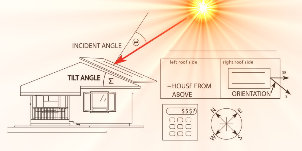
solar panels on a roof that is at least partially facing south (south south-east or south-west)
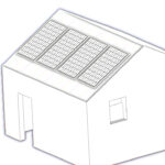
Mini solar power plant
Small solar power plant located on the backyard or any unused land.
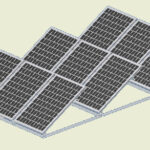
One axis tracker
Adjusting the panel by rotating around one axis is done depending on the day of the month or the month of the year. For this purpose, we need the altitude angle data that SPAC calculate by on the latitude of your installation location. This panel can stand completely horizontally in the case of cloudy weather when only the diffuse radiation component is used. Settings can be done manually or automatically.
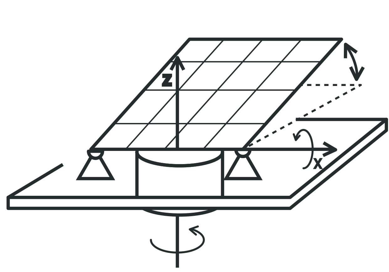
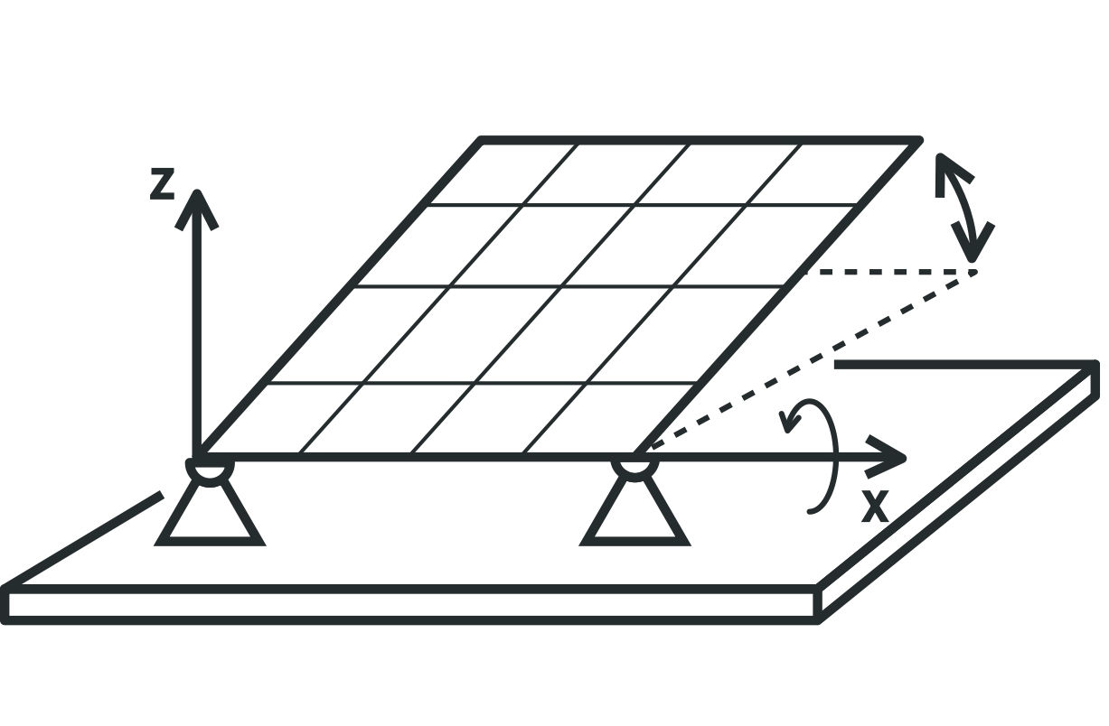
Sun follow panel, two axis tracking
The sun follow panel has a much higher efficiency, but also a more complicated tracking system which requires rotation around the vertical axis depending on the time - the hour angle. The rest is similar as one axis adjustment system. So its adjusments depends from date and time and couldnt be done manualy.
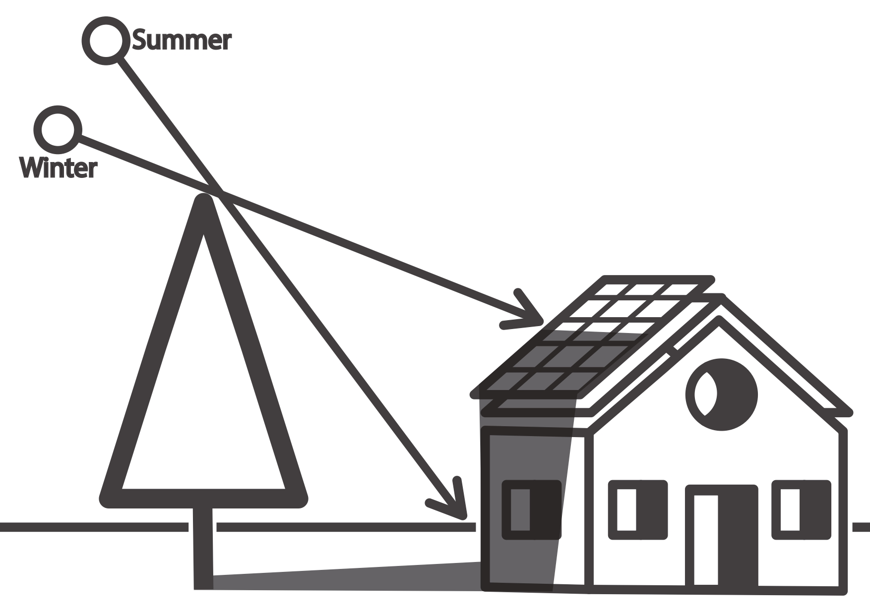
The harmful influence of surrounding objects
Trees, surrounding houses, or any nearby objects that exceed the level of the solar panel can have a harmful effect by casting a shadow, especially in winter.
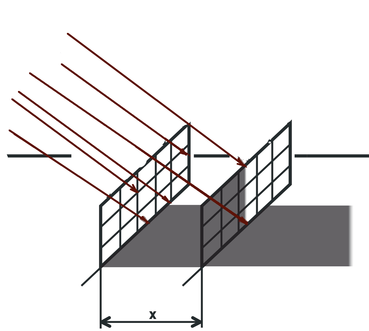
Improper solar panels distance
If solar panels are placed too close to solar power plants, a shadow effect may occur, where one panel partially obscures the other