By the term “pure” semiconductor, we mean semiconductors that do not contain impurities of other elements apart from the basic material.
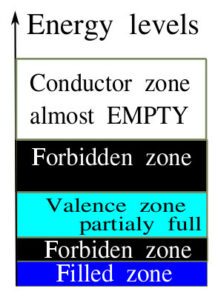
Pure semiconductors have a filled valence zone and an empty conduction zone.
They also have a so-called “forbidden zone.”
The width of that zone is from 1 to 3 eV.
Let’s explain a little of these rough concepts.
Short explanation:
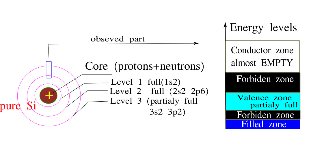
Electrons surround the nucleus of an atom and are grouped at different levels—energy zones.
The valence band is the last energy band filled with electrons in an atom.
The forbidden zone, or energy gap, is a space where electrons cannot be found.
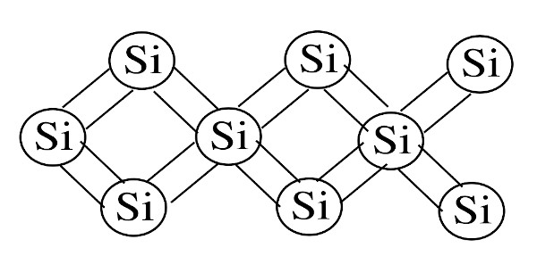
Silicon molecules consist of atoms that form a cubic lattice through covalent bonds. Two electrons (a double bond) are present in the bond between silicon atoms. In silicon molecules without impurity at absolute zero, all electrons are in the valence band, and silicon behaves as an insulator. The energy required to break the covalent bond, also known as the energy of the gap or the energy of the forbidden zone, is 1.1 eV.
Holes
When the valence electron (farthest from the atom’s nucleus) escapes into the conduction zone, an empty space known as a “hole” is created. It then behaves as a carrier of positive charge. The cavity moves from atom to atom as the runaway electron moves. Thus, the illusion is created that the positive charge moves in the opposite direction from the electron’s movement.
pure Si moleculs crystal cell
Energy zones at the end of the Si athom in molecule
Semiconductors with impurities
These are semi-conductors that have been deliberately impurified in the form of a special chemical element, and we will see why. This impuritification is called doping.
More about doping semiconuctor can be found on Wiki
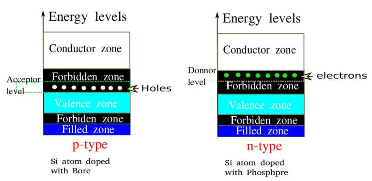
p-type semiconducors
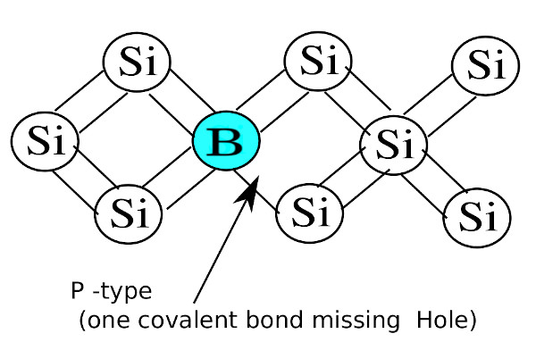
If we replace one silicon atom in the crystal lattice with an atom of boron, gallium, indium, or aluminum (all mentioned have three valence electrons), one covalent bond of silicon would remain unused.
The lack of one electron can be thought of as a hole or as an excess of one positive charge. The energy level of the cavity is higher than the upper limit of the valence band in undoped silicon by only 0.01 eV.
The resulting holes in the valence zone participate in conducting current through the primary semiconductor by transferring ionized energy in the opposite direction from the direction of electron movement.
Acceptors.
Since impenetrable atoms accept excited electrons from the valence band, they are called “acceptors” . And now that we have briefly explained this chemical process, we can define p-type semiconductors as:
Semiconductors with dopers that form holes or positive charges are p-type semiconductors.
n-type Solar tutorials
p-type
n-type semiconductors
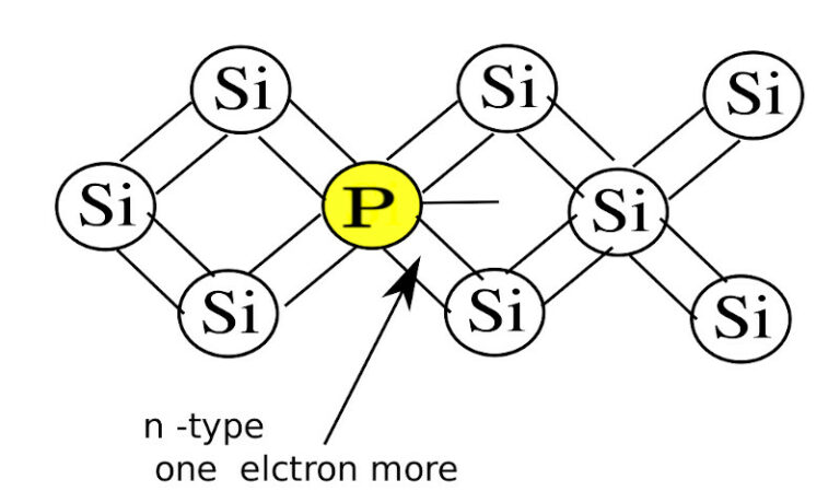
If we were to replace one silicon atom in the crystal lattice with an atom of phosphorus, arsenic, or antimony that has five valence electrons.
Four electrons would be spent on building valence bonds with the surrounding silicon atoms, and one electron would remain attached to the doped element. The energy level of doped elements is located in the upper part of the forbidden zone of the silicon atom and in the immediate vicinity of its conductive zone. If an energy of 0.01 eV is added to these weakly bound electrons, they will move into the conduction zone and participate in the conduction of current through the p-type semiconductor.
Semiconductors with dopers that form free elctron or negative charges are n-type semiconductors.
Energy zones in p-type and n-type semiconducters
Fermi level
The Fermi level is a specific energy level. It is a very important term when connecting p-type semiconductors with n-type semiconductors, i.e., when forming a solar cell.
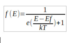
Fermi and Dirac provided a statistical formula for the probability that an electron will be at a particular energy level, signed “E”.
This statistical function contains variables and constant
Ef – Fermi energy level;
k – Boltzmann’s constan
T – temperature (K)
Fermy statistical function
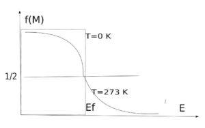
The Fermi energy level is the level of probability of finding electrons equal to 0.5, or it is defined as the highest level at which electrons can be found at a temperature of 0 K (absolute zero).
The dependence of the Fermi function on electron energy and temperature is given in the figure diagram analysis.
For T = 0 K and for E < Ef, the probability of finding an electron at this level is equal to 1. For E>Ef, this probability is 0.
or
For T = 0 K and for E < Ef, all energy level are filled and for E>Ef, all energy levels are empty
As the temperature increases, the number of electrons that can be found at energy levels higher than Ep increases.
In ipure semiconductors (without additional elements), the Fermi level is in the middle.
For p-type semiconductors in the lower part of the forbidden zone. for n-type semiconductors in the upper part of the forbidden zone.
The position of the Fermi level in doped semiconductors depends on the amount of electrons obtained from the p-type impurity and on the temperature. In a state of thermal equilibrium, this level is constant.
Note: This was a very simple explanation. Read more about Fermy levels on Wiki
Solar cells history and rough information you can read here