You are currently viewing p n junction solar cell

p n junction solar cell

lesson 2

In this tutorial, I will explain what happens when p-type and n-type semiconductors are connected.

Dynamics of the p-n junction

First, let’s look at the schematic representation of a p-n junction.

The Fermi level of p-type semiconductors is lower than the Fermi level of n-type semiconductors. It is closer to the nucleus of the atom. There are holes in the lower part of the p-type valence zone. Electrons are located in the lower part of the n-type conduction zone.

When two semiconductors, one of which is n-type and the other p-type, are connected, the transition of holes from p to n semiconductors and electrons from n to p semiconductors occurs. This spontaneous movement of electrons and holes upon joining is known as “diffusion current.” Due to the diffuse movement of electrification on the p-n junction, a thin layer of “transition area,” “transistion field,” or area of the space charge is formed, which is negatively charged on the p-type side and positively charged on the n-type side. This charge redistribution leads to the appearance of an internal electric field and a “contact potential” between the p and n semiconductors.

Under its action, further diffusion of electrons and holes through the thin transition region stops. This further leads to a rise in the energy levels of the p-type and a lowering of the energy level of the n-type semiconductor.

Begginng of p juncion. Fermi level egualization
begginng od junction: Diffuse current and forming inner electric field

Formation of current-voltage characteristics

An important property of the p-n junction is its “rectificationeffect.

A p-n junction conducts current well when the p side is connected to the positive and the n side to the negative pole of the current source. This is called “direct polarization.”

If we connected the p-type to the positive side and the n-type to the negative, we would get a weak movement of electrons (current conduction). This case is called “inverse polarization.” When directly connected to the circuit, the potential barrier is reduced in the transition area. As the voltage increases further, the current increases exponentially. When the p-n junction is connected inverse, the potential barrier and current flow resistance increase in the transition region. With a further increase in voltage, this current reaches a constant value—the “inverse saturation current.” Its value is 10–9 A for silicon.

Elestrong, holes and inner electric field in p n junction
Junction current and voltage

p n junction current Ij

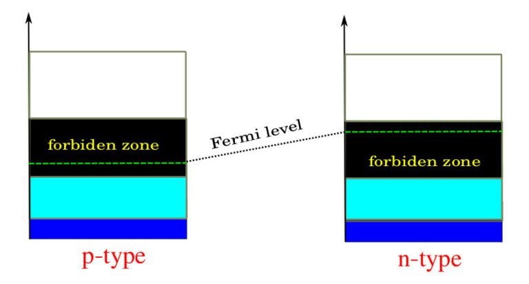
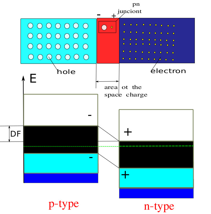
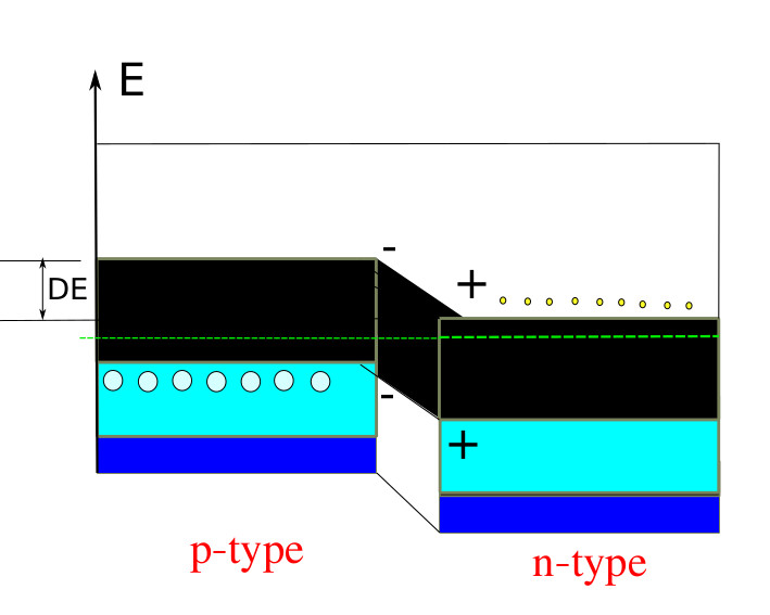
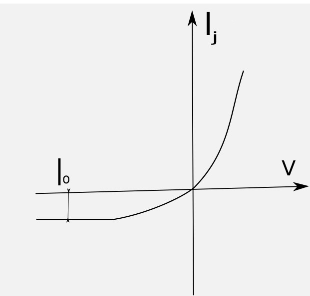
In the p-n junction, the electric current I<sub>j</sub> flows from all carriers of electrification and goes from the p-type to the n-type junction.

We distinguish “minority” and “majority” charge carriers.

The minority charge carriers are electrons on the p side and holes on the n side.

They easily pass through the p-n layer because electrons move down and holes move up in the energy diagram of the p-n junction without interference.

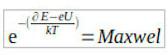
The majority of charge carriers (holes on the p side and electrons on the n side) cannot pass through the p-n junction until their energy becomes greater than.

dE-eUThe majority of charge carriers obey Maxwell’s distribution, which says:

maxwell distributionIn order to find an expression for calculating the current I<sub>j</sub> flowing through the p-n junction, the following notations are introduced:

ul class=”editor-ul”>
  • n1: Number of electrons per unit area on the p side
  • n2: Number of holes per unit area on the p-side
  • n3: Number of electrons per unit area on the n-th side
  • n4: Number of holes per unit area on the n-th side
  • I1: Current of electrons moving from p to n
  • I2: Holes current moving from p to n
  • I3: Electron current moving from n to p
  • I4: Holes current moving from n to p.

k1, k2, k3, and k4 are constants.

I1 = k1 * n1;

I2 = k2 * n2 * Maxwell

I3 = k3*n3*Maxwell

I4 = k4*n4

This is the main formula for further analysis:

Ij = I1 + I2 + I3 + I4 = -(k1*n1 +k4*n4) + (k3*n3 + k2*n2) * Maxwel

I1 = k1 * n1;

I2 = k2 * n2 * Maxwell

I3 = k3*n3*Maxwell

I4 = k4*n4

This is the main formula for further analysis:

Ij = I1 + I2 + I3 + I4 = -(k1*n1 +k4*n4) + (k3*n3 + k2*n2) * Maxwel

p n junction case study

When the p-n junction is not illuminated

If the p-n junction is not illuminated (U = 0 . Ij =0) we can write the expression for the current

k1*n1 + k4*n4 = (k2*n2 + k3*n3) * Maxwell.

For negative voltage values, the main formula is:

Ij = – (k1 * n1 + k4 * n4) = -Io

This means that at large values of negative voltage, the movement of the majority of charge carriers will stop and saturation current will flow. Based on the main formula and the formula for an unilluminated solar cell (p-n junction), we get the formula for the current: Ij = Io * (Maxwel -1)

Conclusion

This was a slightly more complicated lesson, but it is the basis for further understanding of the working principle of a solar cell.

Next lesson : Solar cells under sun light  Previous : p-type n-type semiconductors

This tutorial has step-by-step explanations. If you want to override the details, go here

Maxwell

XIX century was the golden age of physics. The famous Scottish physicist James Clark Maxwell made research in many fields especially electromagnetic. More about this genius you can fihd here..

mmitic

Mechanikal engineer and php programer, work in electric power industry more then25 years

Leave a Reply